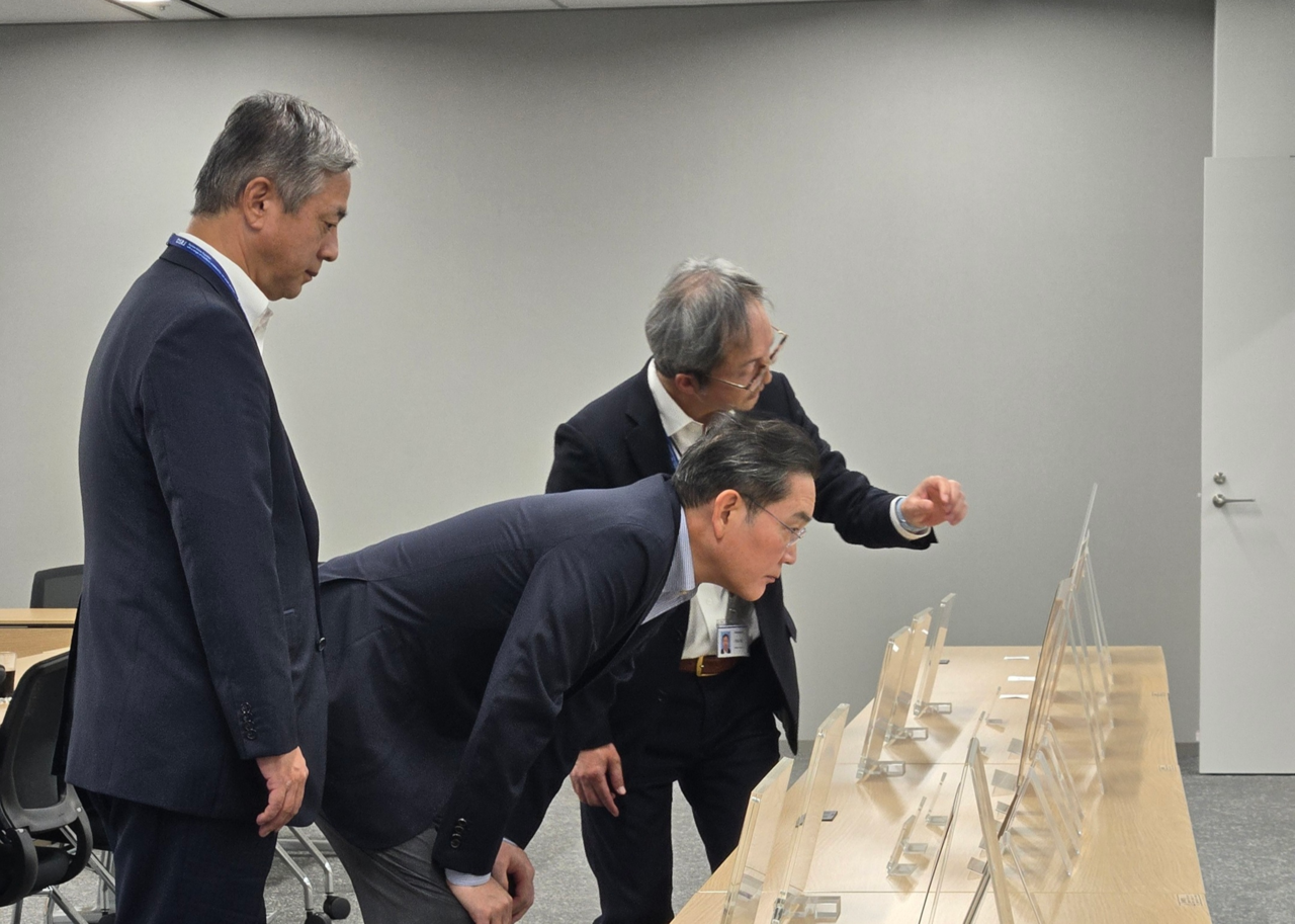

Samsung Electronics Executive Chair Lee Jae-yong visited the company’s advanced semiconductor packaging research facility in Japan on Sunday, emphasizing the need to secure cutting-edge packaging technologies to sharpen its competitive edge in AI chips. Lee inspected the Advanced Package Lab in Yokohama, where he reviewed progress in developing next-generation packaging materials and manufacturing processes with local researchers. He also discussed ways to strengthen cooperation with Japan’s sem